
Oct 4, 2026Applications
Gold Plating for Electronics: Connectors and Lead Frames
Gold plating on contacts and lead frames buys stable, low-resistance, wire-bondable surfaces. See where gold earns its cost and how lines control thickness.
Gold earns its cost only where electrons cross a contact for years: lowest, most stable contact resistance and bondability — bought in microns and controlled by the metre. About a 6-minute read.
Written by Jason Han · Engineering reviewed by Eayon · Published 4 October 2026 · Updated 4 October 2026
Gold plating in electronics is a precision decision, not a luxury decision. On connectors, contacts and lead frames, a micrometre-scale gold layer delivers what no cheaper metal can guarantee over years of mating cycles and thermal aging: near-zero and stable contact resistance, plus wire-bondability where the assembly needs it.
Where Gold Earns Its Cost
- Connector contacts — mating cycles, low insertion-force wear and stable resistance: hard gold (gold alloyed for wear) over a nickel barrier is the classic stack.
- Lead frames and component leads — solderability plus bondability for downstream assembly.
- Wire-bondable pads — soft, high-purity gold (≥99.99% for bonding applications) where aluminium or gold wires bond directly; engineering gold coatings are specified in ASTM B488 (≥99.0% gold for engineering uses, with hardness types).
- PCB final finishes — ENIG/ENEPIG (defined in IPC-4552 and the companion specs, compared in ENIG and ENEPIG) bring gold to the board surface where the circuit, not the connector, needs it.
Where none of those apply, the honest answer is the cheaper finish: tin plating covers most low-current, low-cycle contacts.
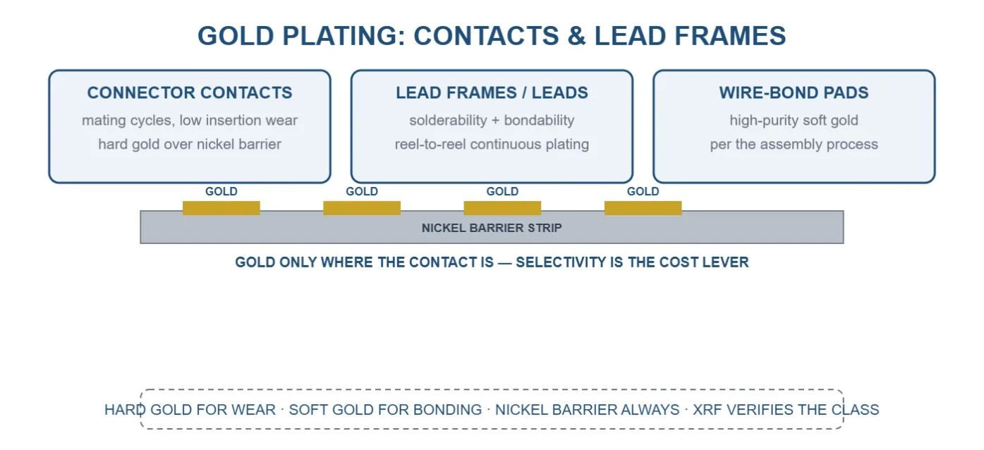
The Stack and the Cost Levers
- Nickel barrier under gold — blocks substrate diffusion, stabilizes resistance; skipping it is the classic reliability mistake.
- Thickness by class — contact specs call out gold thickness classes; more gold than the class is wasted cost, less is a spec miss. XRF measurement (per thickness testing) is the standard QC.
- Selectivity — gold only where the contact zone needs it: spot/stripe plating on reel-to-reel lines, masked racks on rack lines. Selectivity is the single biggest cost lever on gold-bearing parts.
- Bath discipline — gold baths run on tight contamination control; drag-out recovery and bath analysis protect both quality and metal accounting.
Equipment That Controls Gold
- Reel-to-reel continuous lines for strips and lead frames — the standard for volume contacts, with inline XRF and selectivity tooling.
- Rack lines for housings and larger contacts — masked fixtures, controlled current density at the contact points.
- VCP lines where PCB panels carry the gold.
- Peripheral accountability — rectifier stability, filtration and precious-metal recovery; the platform base is under plating lines.

Field Workflow: Spec Gold in Five Questions
- ☐ Contact function — mating cycles, bonding, or solderability?
- ☐ Gold type — hard gold (wear) or high-purity soft gold (bonding)?
- ☐ Thickness class and measurement points on the part
- ☐ Underlayer stack — nickel barrier present?
- ☐ Format — reel, rack or panel, and where selectivity can cut cost
Standards and Evidence Boundary
- ASTM B488 — standard specification for electrodeposited coatings of gold for engineering uses — ASTM International.
- IPC-4552 — performance specification for ENIG plating for printed circuit boards — IPC.
- IPC-4556 — performance specification for ENEPIG plating for printed circuit boards — IPC.
Evidence boundary: this article covers gold plating at industry-general level. Thickness classes, bondability acceptance and bath windows come from your drawings, the applicable specifications and the chemistry supplier — not from this page.
FAQ
Hard gold vs soft gold — what is the difference in practice?
Hard gold (alloyed, often with cobalt or nickel) resists wear for mating contacts; soft high-purity gold deforms and bonds — for wire bonding. The assembly decides which surface the part needs.
Why is a nickel barrier mandatory under gold?
Substrate atoms diffuse through thin gold over time, oxidizing the surface and destroying contact resistance and bondability. Nickel stops that diffusion and stabilizes the interface.
Can gold thickness be reduced by better design?
Yes — selectivity (plate only the contact zone), contact geometry, and honest thickness classes from the spec are the three levers. Geometry and spec review pay more than chemistry tuning.
Is ENIG the same as gold plating?
Different process: ENIG is a displacement (immersion) finish applied to the board in the PCB plant; electrolytic gold plating deposits controlled thicknesses on connectors, frames and pads in a plating line. They meet at the assembly.
Related Reading
- Finish family: ENEPIG vs ENIG: PCB Surface Finishes Compared — the board-side gold finishes.
- Alternative: Tin Plating for Electronics & Bus Bars — the economical contact metal.
- Next step: browse plating lines including reel-to-reel and selective configurations.
Diagnostic CTA: What to Send Us — and What You Get Back
Send three inputs through our RFQ form:
- The contact parts, their function and gold spec (type, thickness class)
- Substrate and underlayer stack
- Format and volume — reel, rack or panel
ES-PRO returns: a line configuration with selectivity and thickness-control design, an equipment list including metal-accounting peripherals, a quotation, and an explicit list of open questions — we state what is missing rather than assuming it.
References & Authorities
- ASTM B488 — Standard specification for electrodeposited coatings of gold for engineering uses — ASTM International.
- IPC-4552 — Performance specification for electroless nickel/immersion gold (ENIG) plating for printed circuit boards — IPC.
- IPC-4556 — Performance specification for electroless nickel/electroless palladium/immersion gold (ENEPIG) plating for printed circuit boards — IPC.
- Chemistry supplier datasheets — bath systems, additives and operating windows for the specific gold chemistry (issued by the chemistry supplier).
- Industry associations — e.g., NASF (National Association for Surface Finishing, US) and IMF (Institute of Materials Finishing, UK) publish supplementary guidance and training for the surface-finishing industry.
- Standards are cited for identification; always use the current edition from the issuing body. Process parameters are governed by the datasheets for the specific chemistry.